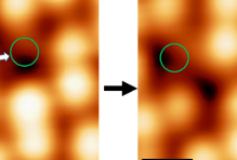
Scientists at the Okinawa Institute of Technology (OIST) in Japan have successfully used scanning tunneling microscopy to observe the nature of structural defects in a perovskite solar cell material.
That defects exist in perovskite materials, and have an adverse effect on their performance as solar cells, has long been known. However, the precise nature of these defects and the resulting mechanisms that affect device stability, is less well understood. Delving into their characteristics, as the OIST group has done, could help to inform the design of future device designs that minimize or even eliminate the influence of such defects.
Many different approaches to this problem have been suggested, including ‘healing’ defects through carefully managed exposure to heat and light, using a potassium solution to limit the ion movement caused by such defects, and inserting extra layers into the cell.
The scientists used scanning tunneling microscopy – a method which looks at the atomic level properties of a surface – to observe in high resolution the movement of individual particles across the surface of the perovskite solar cell based on methylammonium lead bromide.
Their analysis of these images, combined with calculations from collaborators at the University of Pittsburgh, demonstrated groups of vacant spaces across the surface, where atoms were missing, and also noticed pairs of bromide ions shifting and changing direction on the surface.

Microscope image showing the movement of ions across the perovskite’s surface. Image: OIST
Image: OIST
In their results, published in ACS Nano, the group concludes that the ‘missing atoms’ on the surface are likely the cause of the shifting bromide atoms. “These perovskite surfaces are much more dynamic than we previously anticipated,” said Stecker. “Now, with these new findings, we hope engineers can better account for the effect of defects and their motion in order to improve devices.”


