Moving perovskite solar cells into commercial production is a focus for many of the world’s leading research institutes, which have a wealth of different approaches, materials and processes to evaluate and work with.
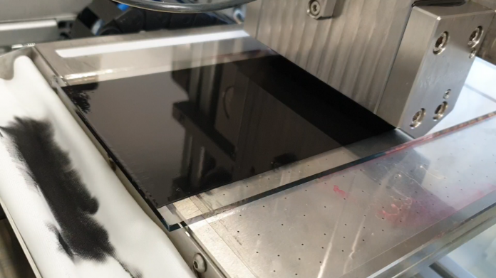
Many of these approaches use variations on slot die coating – a process already proven in several other industries, in which a liquid is coated onto a substrate via a thin slot positioned close to the substrate, to deposit the layers needed for the solar cell. Others have looked to inkjet printing processes. Slot die coating though is said to be faster and more effective in ensuring uniform thickness of the layers.
The process developed by EMPA, working in conjunction with fellow Swiss company Solaronix, deposits layers using slot die coating, and then structures the layers, removing excess material with a laser. This allows even more flexibility in determining the thickness of the layers, according to Frank Nüesch, head of EMPA’s functional polymers department.
Five layers
EMPA also notes that with its slot die coating process, four of the five cell layers (graphite, titanium oxide, zirconium and a conductive oxide) can all applied one after the other, a further advantage over inkjet processes, which require each layer to be individually dried and compacted before the next is applied. The perovskite absorber is then applied using an inkjet process, and seeps through the porous cell layers to the bottom.

As proof of concept for the process, the laboratory has produced a functioning perovskite solar cell with a surface area of 10x10cm. EMPA claims the cells produced using its process boast “a longer service life compared to previous perovskite cells,” and says it has plans to prove this in field testing, with plans in place to install test arrays the cells on rooftops at its campus in Dübendorf, Switzerland.


