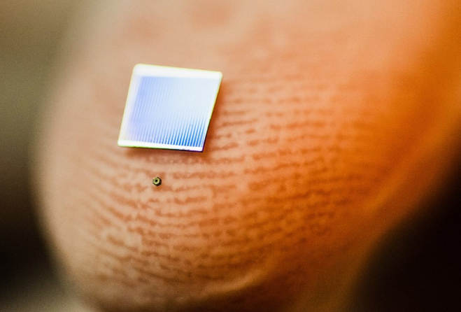
A French-Canadian research team has recently developed a micrometer-scale triple-junction III-V solar cell for applications in concentrated photovoltaics (CPV).
The device is based on indium gallium phosphide (InGaP), indium gallium arsenide (InGaAs) and germanium (Ge) and has an active area of only 0.089 mm2. “We have not included these cells into real modules yet,” Sherbrooke Professor, Maxime Darnon, told pv magazine. “We would be happy to collaborate with any group that would need such cells.”
According to him, the processes used to fabricate the cells are almost identical to the processes used for conventional III-V cells, such as those produced by German specialist Azur Space, except for the isolation and dicing process that is plasma-based, while in other cells for CPV applications saw dicing in commonly used. “It is hard to anticipate the exact cost in production conditions, but we can say that mm2 cells fabricated with plasma etching would be approximately the same price as cells fabricated with saw dicing, and for micrometer-scale solar cells, plasma etching is the only economically viable solution since we waste much less valuable material with plasma etching than with saw dicing,” he further explained.
The cell was designed with rectangular, circular, and hexagonal active areas and built with a commercial epitaxial germanium wafer and titanium-aluminum (Ti/Al) metallization deposited on the backside of the wafer. An anti-reflective coating (ARC) made of silicon nitride hydrogen (SiNxHy) and hydrogenated silicon oxide (SiOxHy) was then deposited by plasma-enhanced chemical vapor deposition (PECVD), which was key to minimize surface recombinations.
Saw dicing was discarded to avoid defect generation due to the fragility of the germanium wafer and the targeted small area of the cell. “In addition, saw dicing generates linear channels that force the fabricated cells to be rectangular, which may be inadequate depending on the incoming light profile,” the researchers explained.
The performance of the micro-scale cell was analyzed under standard AM1.5G sunlight conditions and the device showed an open-circuit voltage of 2.350 V, a short-circuit current density of 12.40 mA cm−2, and a fill factor of 82.7%. “However, a degradation of the electrical performance was observed when reducing cell areas with up to 10.2% drop in open-circuit voltage for cells without passivating ARC,” the research team noted.
The scientists achieved the maximum efficiency of 34.4% for a 1-mm2 cell under concentrated light of 450 suns and of 33.8% under 584 suns for a 0.25-mm2 device. “Lower current and lower series resistance in smaller cells are expected to shift the maximum efficiency to higher concentration,” they further explained.
The micrometer-scale cell is presented in the paper Miniaturization of InGaP/InGaAs/Ge solar cells for micro‐concentrator photovoltaics, published in Progress in Photovoltaics. The research group includes scientists from the Université de Sherbrooke and the University of Ottawa in Canada, the French National Centre for Scientific Research (CNRS), the University of Bordeaux in France.
The wrok was performed conjointly at the Laboratoire Nanotechnologies Nanosystèmes ([labn2.ca]LN2) and Laboratoire d’Intégration du Matériau au Système (IMS). The research project was funded by the Natural Sciences and Engineering Research Council of Canada (NSERC), Prompt, a Canadian non-profit organization dedicated to facilitating partnerships and R & D financing between businesses and the public research sector, and Canada-based industrial partner Saint-Augustin Canada Electric inc. (STACE).
The cost of producing solar cells based on compounds of III-V element materials–named according to the groups of the periodic table that they belong to–has confined such devices to niche applications including drones and satellites, where low weight and high efficiency are more pressing concerns than costs, in relation to the energy produced.


