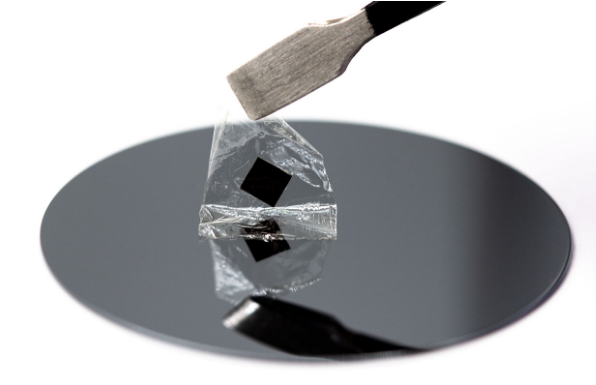
Even as perovskite solar cells move toward commercial production, the class of materials offers many more possibilities that remain confined to academia for now. Single-crystal perovskites are one example of this.
For the polycrystalline perovskites that have made it further down the path to commercialization, the potential for simple low-cost production processes is one of the main attractions. Single-crystal perovskites offer potential advantages over these, in terms of both performance and stability, but are more challenging to fabricate and so have not seen the same level of commercial interest.
A group of scientists led by University of California San Diego (UCSD) investigated this, and has developed a process based on lithography and other processes already used elsewhere in manufacturing, to produce a single-crystal perovskite film.
“Our method is the first that can precisely control the growth and fabrication of single-crystal devices with high efficiency,” says Yusheng Lei, a graduate student in nano-engineering at UCSD. “The method doesn’t require fancy equipment or techniques – the whole process is based on traditional semiconductor fabrication, further indicating its compatibility with existing industrial procedures.”
They describe the process in “A fabrication process for flexible single-crystal perovskite devices,” which was recently published in Nature. The group was able to fabricate continuous monocrystalline thin films up to a size of around 5.5cm x 5.5cm, with precise control over the thickness from around 0.6 to 100 micrometers.
Different tests
The group produced graded flexible thin films with varying mixtures of lead and tin, and when integrated into solar cells, they achieved an overall efficiency of around 10.3%. The group further noted that these could be improved with strategic layer designs and passivation.
The flexible perovskite thin-films were also subjected to mechanical stress and various light intensities, temperatures, and humidity levels. In these tests, they demonstrated strong performance in comparison to polycrystalline perovskite materials.
“Single-crystal devices show a slower decay than polycrystalline devices with the same measurement conditions and encapsulation in 1,000-h continuous illumination stability tests under 1-sun intensity by tracking the maximum power point,” the scientists said. Evidence also suggests that the grain boundaries between crystals are major contributors to their degradation.
The group has stated that its research serves as proof that single-crystal perovskite devices can be made using industry-standard processes and materials. It plans to continue work on this process with a view to eventually reaching commercial scale.
“Further simplifying the fabrication process and improving the transfer yield are urgent issues we’re working on,” says Sheng Xu, a professor in UCSD’s Department of Nanoengineering. “Alternatively, if we can replace the pattern mask with functional carrier transport layers to avoid the transfer step, the whole fabrication yield can be largely improved.”
A step forward for single-crystal perovskites
Scientists in the United States have developed a lithography-based process for the fabrication of single-crystal perovskites. Thin films made using this process have been integrated into a range of devices, including solar cells, and have demonstrated better stability performance than their more commonly researched polycrystalline counterparts.
Source:PV magazine


